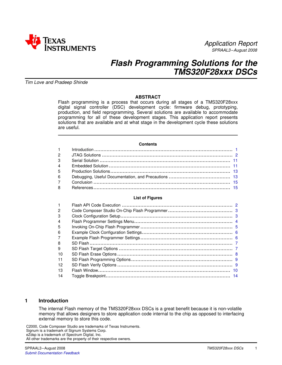
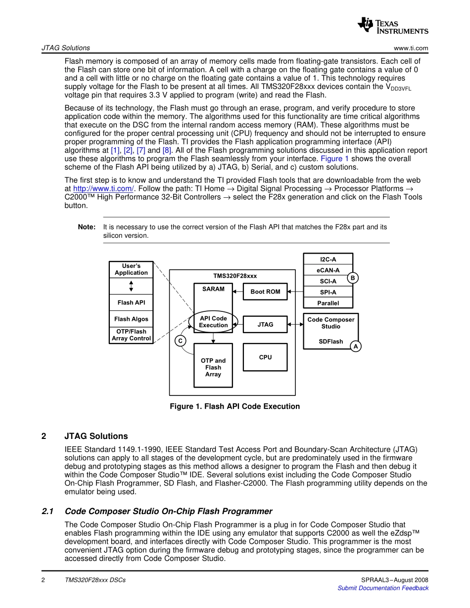
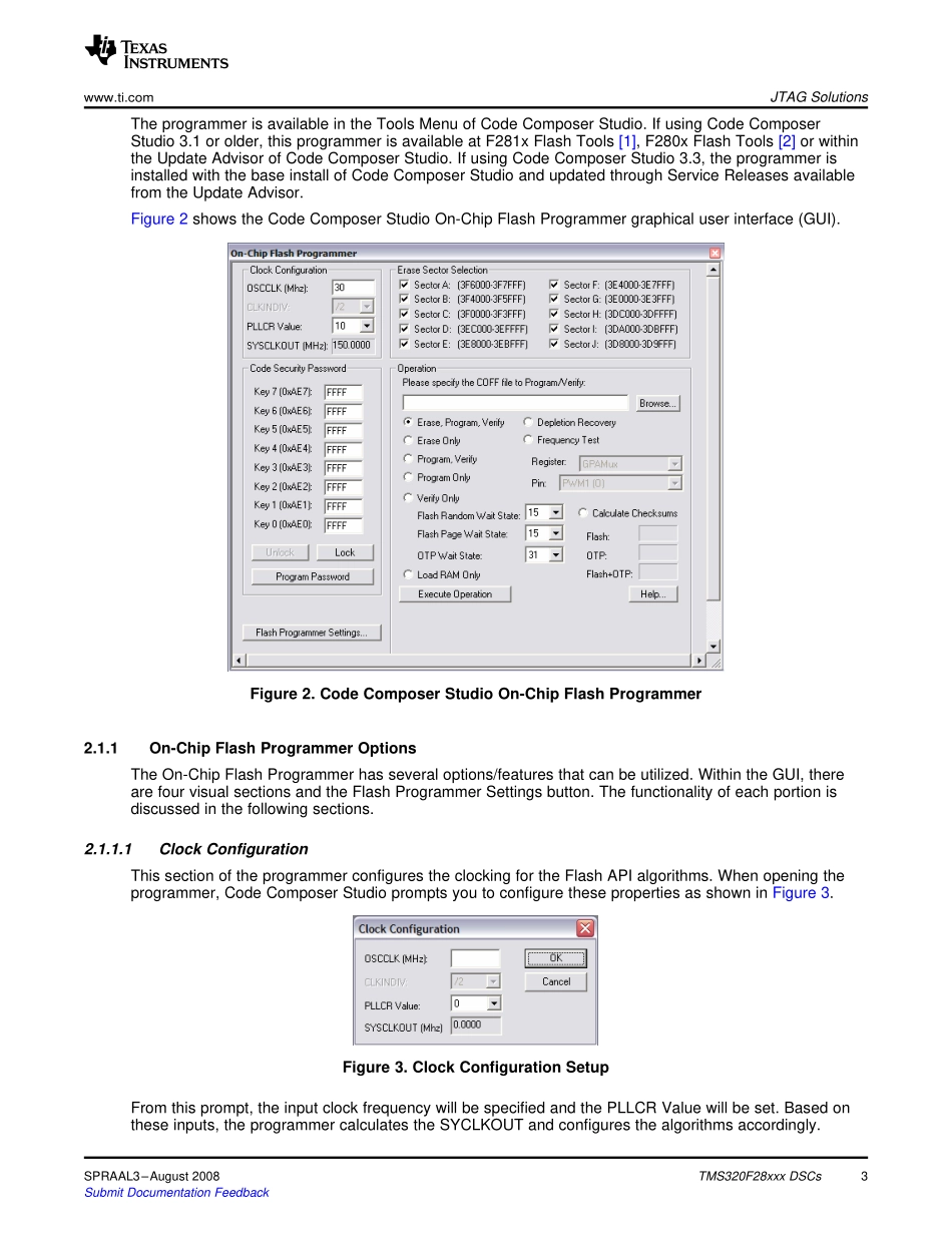
分享
Flash_Programming_spraal3.pdf
下载文档

ID:3519063

大小:423.85KB

页数:16页

格式:PDF

时间:2024-05-18

收藏 分享赚钱
温馨提示:
1. 部分包含数学公式或PPT动画的文件,查看预览时可能会显示错乱或异常,文件下载后无此问题,请放心下载。
2. 本文档由用户上传,版权归属用户,汇文网负责整理代发布。如果您对本文档版权有争议请及时联系客服。
3. 下载前请仔细阅读文档内容,确认文档内容符合您的需求后进行下载,若出现内容与标题不符可向本站投诉处理。
4. 下载文档时可能由于网络波动等原因无法下载或下载错误,付费完成后未能成功下载的用户请联系客服处理。
网站客服:3074922707
Flash_Programming_spraal3
1IntroductionApplication ReportSPRAAL3August 2008Flash Programming Solutions for theTMS320F28xxx DSCsTim Love and Pradeep Shinde.ABSTRACTFlash programming is a process that occurs during all stages of a TMS320F28xxxdigitalsignalcontroller(DSC)developmentcycle:firmwaredebug,prototyping,production,and field reprogramming.Several solutions are available to accommodateprogramming for all of these development stages.This application report presentssolutions that are available and at what stage in the development cycle these solutionsare useful.Contents1Introduction.12JTAG Solutions.23Serial Solution.114Embedded Solution.115Production Solutions.136Debugging,Useful Documentation,and Precautions.137Conclusion.158References.15List of Figures1Flash API Code Execution.22Code Composer Studio On-Chip Flash Programmer.33Clock Configuration Setup.34Flash Programmer Settings Menu.45Invoking On-Chip Flash Programmer.56Example Clock Configuration Settings.67Example Flash Programmer Settings.68SD Flash.79SD Flash Target Options.710SD Flash Erase Options.811SD Flash Programming Options.912SD Flash Verify Options.913Flash Window.1014Toggle Breakpoint.14The internal Flash memory of the TMS320F28xxx DSCs is a great benefit because it is non-volatilememory that allows designers to store application code internal to the chip as opposed to interfacingexternal memory to store this code.C2000,Code Composer Studio are trademarks of Texas Instruments.Signum is a trademark of Signum Systems Corp.eZdsp is a trademark of Spectrum Digital,Inc.All other trademarks are the property of their respective owners.SPRAAL3August 2008TMS320F28xxx DSCs1Submit Documentation FeedbackUsersApplicationFlash APIFlash AlgosOTP/FlashArray?ControlBoot?ROMJTAGSARAMAPI?CodeExecutionOTP andFlashArrayCPUCTMS320F28xxxI2C-AeCAN-ASCI-AParallelCode?ComposerStudioSDFlashBASPI-A2JTAG Solutions2.1Code Composer Studio On-Chip Flash ProgrammerJTAG SFlash memory is composed of an array of memory cells made from floating-gate transistors.Each cell ofthe Flash can store one bit of information.A cell with a charge on the floating gate contains a value of 0and a cell with little or no charge on the floating gate contains a value of 1.This technology requiressupply voltage for the Flash to be present at all times.All TMS320F28xxx devices contain the VDD3VFLvoltage pin that requires 3.3 V applied to program(write)and read the Flash.Because of its technology,the Flash must go through an erase,program,and verify procedure to storeapplication code within the memory.The algorithms used for this functionality are time critical algorithmsthat execute on the DSC from the internal random access memory(RAM).These algorithms must beconfigured for the proper central processing unit(CPU)frequency and should not be interrupted to ensureproper programming of the Flash.TI provides the Flash application programming interface(API)algorithms at 1,2,7 and 8.All of the Flash programming solutions discussed in this application reportuse these algorithms to program the Flash seamlessly from your interface.Figure 1 shows the overallscheme of the Flash API being utilized by a)JTAG,b)Serial,and c)custom solutions.The first step is to know and understand the TI provided Flash tools that are downloadable from the webat http:/ the path:TI Home Digital Signal Processing Processor Platforms C2000 High Performance 32-Bit Controllers select the F28x generation and click on the Flash Toolsbutton.Note:It is necessary to use the correct version of the Flash API that matches the F28x part and itssilicon version.Figure 1.Flash API Code ExecutionIEEE Standard 1149.1-1990,IEEE Standard Test Access Port and Boundary-Scan Architecture(JTAG)solutions can apply to all stages of the development cycle,but are predominately used in the firmwaredebug and prototyping stages as this method allows a designer to program the Flash and then debug itwithin the Code Composer Studio IDE.Several solutions exist including the Code Composer StudioOn-Chip Flash Programmer,SD Flash,and Flasher-C2000.The Flash programming utility depends on theemulator being used.The Code Composer Studio On-Chip Flash Programmer is a plug in for Code Composer Studio thatenables Flash programming within the IDE using any emulator that supports C2000 as well the eZdspdevelopment board,and interfaces directly with Code Composer Studio.This programmer is the mostconvenient JTAG option during the firmware debug and prototyping stages,since the programmer can beaccessed directly from Code Composer Studio.2TMS320F28xxx DSCsSPRAAL3August 2008Submit Documentation Feedback2.1.1On-Chip Flash Programmer Options2.1.1.1Clock CJTAG SolutionsThe programmer is available in the Tools Menu of Code Composer Studio.If using Code ComposerStudio 3.1 or older,this programmer is available at F281x Flash Tools 1,F280 x Flash Tools 2 or withinthe Update Advisor of Code Composer Studio.If using Code Composer Studio 3.3,the programmer isinstalled with the base install of Code Composer Studio and updated through Service Releases availablefrom the Update Advisor.Figure 2 shows the Code Composer Studio On-Chip Flash Programmer graphical user interface(GUI).Figure 2.Code Composer Studio On-Chip Flash ProgrammerThe On-Chip Flash Programmer has several options/features that can be utilized.Within the GUI,thereare four visual sections and the Flash Programmer Settings button.The functionality of each portion isdiscussed in the following sections.This section of the programmer configures the clocking for the Flash API algorithms.When opening theprogrammer,Code Composer Studio prompts you to configure these properties as shown in Figure 3.Figure 3.Clock Configuration SetupFrom this prompt,the input clock frequency will be specified and the PLLCR Value will be set.Based onthese inputs,the programmer calculates the SYCLKOUT and configures the algorithms accordingly.SPRAAL3August 2008TMS320F28xxx DSCs3Submit Documentation Feedback2.1.1.2Flash Programmer Settings2.1.1.3Erase Sector Selection2.1.1.4OperationJTAG SThe Flash Programmer Settings button opens the menu shown in Figure 4.Figure 4.Flash Programmer Settings MenuThe Flash API file is selected from this menu.When selecting this algorithm,the Browse button navigatesyou to the algorithms available on the system.Always choose the most recent algorithm.The device can be selected from this menu.This defaults to the device that Code Composer Studio isconfigured for.The other options available are:Load Symbols-Enables/Disables Code Composer Studio to Load Symbols directly after programmingFlash to enable debugging.Display Tooltips Enables/Disables details within the programmer when hovering over an option.Display Diagnostics Enables/Disables output screen that displays the status of programming.Save Clock Settings Enables/Disables the option to save the clock settings entered inSection 2.1.1.1.This section of the programmer allows you to select all or just certain sections of the Flash memory toerase.This option is helpful because it allows sectors to keep their contents if there is code programmedto that sector that should not be erased.Unused sectors can be deselected and will not be erased,whichis also beneficial for decreasing overall erase time.The operation portion of the programmer contains several features:Specifying a COFF File The.out file to program to the Flash is input in this section.If a project isopen and built in Code Composer Studio,the resulting.out file is automatically specified.Erase,Program,and Verify Operations These buttons allow the erase,program,and verifyoperations to simultaneously run or execute each operation individually.Depletion Recovery This option invokes the depletion recovery algorithm that looks for sectors thatare in depletion and attempts to recover them.Frequency Test The clock configuration specified from Section 2.1.1.1 can be verified on thegeneral-purpose input/output(GPIO)pin of choice.Calculate Checksums Performs a checksum of the Flash,one-time programmable(OTP),and Flash+OTP.Load RAM Only This option loads initialized sections that are specified to run from RAM.Wait States During programming,the Wait States for the Flash and OTP are set with these options.Execute Operation This button will execute whatever option is selected.Help This button will open the Help Files with all documentation associated for the programmer.TMS320F28xxx DSCs4SPRAAL3August 2008Submit Documentation Feedback2.1.1.5Code Security Password2.1.2Programming EJTAG SolutionsThe Code Security Password portion of the programmer directly accesses the Code Security Module(CSM)of the Flash memory.The CSM consists of eight 16-bit memory locations that enables the Flash tobe password protected.For complete details regarding the CSM,see the Code Security Module(CSM)section of 10,11 and 12.This portion of the programmer contains the following elements:KEY0 KEY7-16-bit password locations.Unlock Unlocks Flash if CSM is secured and passwords are written in KEY0 KEY7.Lock Locks the Flash if the CSM has previously been programmed with the passwords written inKEY0 KEY7.Program Password Programs the passwords to the CSM that is written in KEY0 KEY7.The Flashis required to be erased for this process.If the Flash has not been erased when the ProgramPassword button is pressed,the Flash Plug In will prompt you to erase the Flash.There are several precautions to be aware of when using the CSM.For further details,see Section 6.3.The process of programming and debugging from the Flash only contains a few steps.For this example,the TMS320F28335 eZdsp,Code Composer Studio 3.3,and Flash example from Running an Applicationfrom Internal Flash Memory on the TMS320F28xxx DSP(SPRA958)3 were used.This process isuniversal for all TMS320F28xxx DSCs.1.Connect the target board to the PC using the JTAG emulator and power the board with the appropriatepower connector.2.Start Code Composer Studio with the appropriate emulation driver selected in the Code ComposerStudio setup utility.3.Open and Build the project by selecting Project Open followed by Project Rebuild All.4.Open the On-Chip Flash Programmer from the Tools Menu.Figure 5.Invoking On-Chip Flash ProgrammerSPRAAL3August 2008TMS320F28xxx DSCs5Submit Documentation Feedback2.2SD FlashJTAG S5.Configure Clock Settings for the target board as described in Section 2.1.1.1.Figure 6.Example Clock Configuration Settings6.Select the correct algorithm for the programmer as described in Section 2.1.1.2.Figure 7.Example Flash Programmer Settings7.Select the sectors that will be erased/programmed as described in Section 2.1.1.3.8.Select Execute Operation as the Erase,Program,Verify option is default and the.out file should bespecified already from building the project.Once this process has finished,the program is stored on the Flash and the board is ready for standaloneoperation or debugging,through Code Composer Studio,by using the method described in Section 6.1.SD Flash is a free,standalone programmer that enables programming with a Spectrum Digital emulatorwithout requiring the need of Code Composer Studio.Because of this,this programmer is useful for alldevelopment stages of a product as well.The utility,algorithms,example projects,and full documentationexplaining how to use the utility are available at the SD Flash Utility home page 4.TMS320F28xxx DSCs6SPRAAL3August 2008Submit Documentation Feedback2.2.1TJTAG SolutionsThe SD Flash GUI is shown in Figure 8.Figure 8.SD FlashSD Flash uses projects to configure all settings for the JTAG connection,erase,programming,and verifyoptions.A new project can be created or an existing project can be opened from the File menu.Once theproject is opened,the settings are configured by selecting Project-Settings.Figure 9 shows the target options.The target tab configures the JTAG connection for the device options.Figure 9.SD Flash Target OptionsThe options within this tab are as follows:Driver Selects the Code Composer Studio emulation driver used to communicate with the device.Emulator Address/ID Selects the address for the JTAG emulator.The default is 0 x378 for theXDS510PP and 510 for XDS510USB.SPRAAL3August 2008TMS320F28xxx DSCs7Submit Documentation Feedback2.2.2EraseJTAG SBoard File-Provides information to the SD Flash regarding the number of devices on the JTAG scanchain.Processor Name Used to place a generic name for the device within the project.Figure 10 shows the erase tab that configures all options for the erase process.Figure 10.SD Flash Erase OptionsThe options within this tab are as follows:Algorithm File Specify erase algorithm for project.The file should be selected for the specific devicebeing used.Timeout Set timeout for the erase process in terms of seconds.User Options 1-Specify which sectors to erase.00FF is default and will specify all sectors.User Options 2/User Options 4 Not Used.User Options 3 Run frequency toggle test.ST0/ST1/PMST/PMST Address Default is blank and should not be used.8TMS320F28xxx DSCsSPRAAL3August 2008Submit Documentation Feedback2.2.3Programming2.2.4VJTAG SolutionsFigure 11 shows the programming tab that configures all options for the programming process.Figure 11.SD Flash Programming OptionsThe options within this tab are as follows:Algorithm File Specify programming algorithm for project.The file should be selected for the specificdevice being used.Flash Data File Specify.out file produced from Code Composer Studio project to program to theFlash.Timeout Set timeout for the programming process in terms of seconds.User Options 3 Run frequency toggle test.User Options 1/User Options 2/User Options 4 Not Used.ST0/ST1/PMST/PMST Address Default is blank and should not be used.Figure 12 shows the verify tab that configures all options for the verify process.Figure 12.SD Flash Verify OptionsSPRAAL3August 2008TMS320F28xxx DSCs9Submit Documentation Feedback2.2.5Programming Example2.3Flasher-C2000JTAG SThe options within this tab are as follows:Algorithm File Specify verify algorithm for project.The file should be selected for the specific devicebeing used.Timeout Set timeout for the verify process in terms of seconds.User Options 1/User Options 2 Specify wait states used for the Flash and OTP during the verifyoperation.User Options 3-Run frequency toggle test.User Options 4 Not Used.ST0/ST1/PMST/PMST Address Default is blank and should not be used.The process of programming the Flash only contains a few steps.For this example,the TMS320F28335eZdsp,SampleF28335usb.sdp(provided SD Flash project),and Flash example from Running anApplication from Internal Flash Memory on the TMS320F28xxx DSP(SPRA958)3 were used.Thisprocess is universal for all TMS320F28xxx DSCs.1.Download the SD Flash utility and algorithms from SD Flash 4.2.Connect the target board to the PC using the JTAG emulator and power the board with the appropriatepower connector.3.Open SD Flash.4.Open the provided SD Flash project file by selecting File Open Project.5.Modify any project options describ

此文档下载收益归作者所有

下载文档
收起
展开