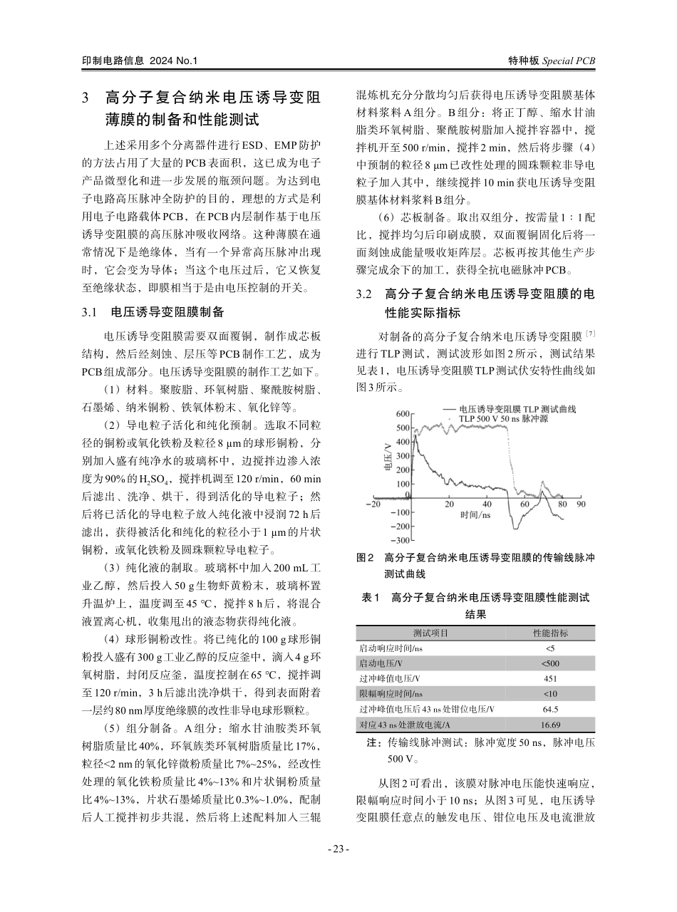
印制电路信息2024No.1特种板SpecialPCB基于高分子电压诱导变阻膜的全PCB抗脉冲防护刘辉1吴丰顺1武占成2龚德权3王晶3胡元伟3马浩轩3(1.华中科技大学材料科学与工程学院,湖北武汉430074;2.中国航天五院五一四所院士专家工作站,北京100086;3.武汉芯宝科技有限公司,湖北武汉430043)摘要随着芯片集成度的不断提高,内部互连导线间距越来越小,器件更易在静电作用下受到损害。为提高印制电路板(PCB)在实际应用中抗静电放电(ESD)和电磁脉冲(EMP)的能力,制作了一种高分子电压诱导变阻膜,将其嵌入PCB中形成脉冲吸收网络,使全板具备抗瞬变脉冲能力,实现对ESD和EMP的全系统防护。ESD防护实测结果表明,对比普通PCB,全抗脉冲PCB对静电脉冲有更快的响应速度和更高的释放效率;传输线脉冲(TLP)测试结果表明,采用电压诱导变阻膜的PCB中每一点都具有过电压脉冲吸收能力,电流泄放能力可达50A以上。关键词静电放电(ESD);传输线脉冲(TLP)测试;电磁脉冲(EMP);变阻膜中图分类号:TN41文献标志码:A文章编号:1009⁃0096(2024)01⁃0021⁃05Anti-pulseprotectionofwholecircuitboardbasedonpolymervoltage-inducedrheostaticfilmLIUHui1WUFengshun1WUZhancheng2GONGDequan3WANGJing3HUYuanwei3MAHaoxuan3(1.SchoolofMaterialsScienceandEngineering,HuazhongUniversityofScienceandTechnology,Wuhan430074,Hubei,China;2.514AcademicianExpertWorkstation,theFifthAcademyofChinaAerospaceScienceandTechnology,Beijing100086,China;3.WuhanChipProtectionTechnologyCo.,Ltd.,Wuhan430043,Hubei,China)AbstractWiththecontinuousimprovementofchipintegration,theinterconnectwirespacingbecomessmallerandsmaller,sothedeviceismorevulnerabletoelectrostaticdamage.Inordertoimprovetheabilityoftheprintedcircuitboard(PCB)toresistelectrostaticdischarge(ESD)andelectromagneticpulse(EMP)inpracticalapplications,apolymervoltage-inducedrheostaticfilmispreparedandembeddedintothePCBtoformapulseabsorptionnetwork,sothattheentirecircuitboardhastheabilitytoresisttransientpulseandrealizethewholesystemprotectionagainstESDandEMP.ThemeasuredresultsofESDprotectionshowthatcomparedwiththeordinarycircuitboard,thefullresistancepulsecircuitboardhasfasterresponsespeedandhigherreleaseefficiencytotheelectrostatic...