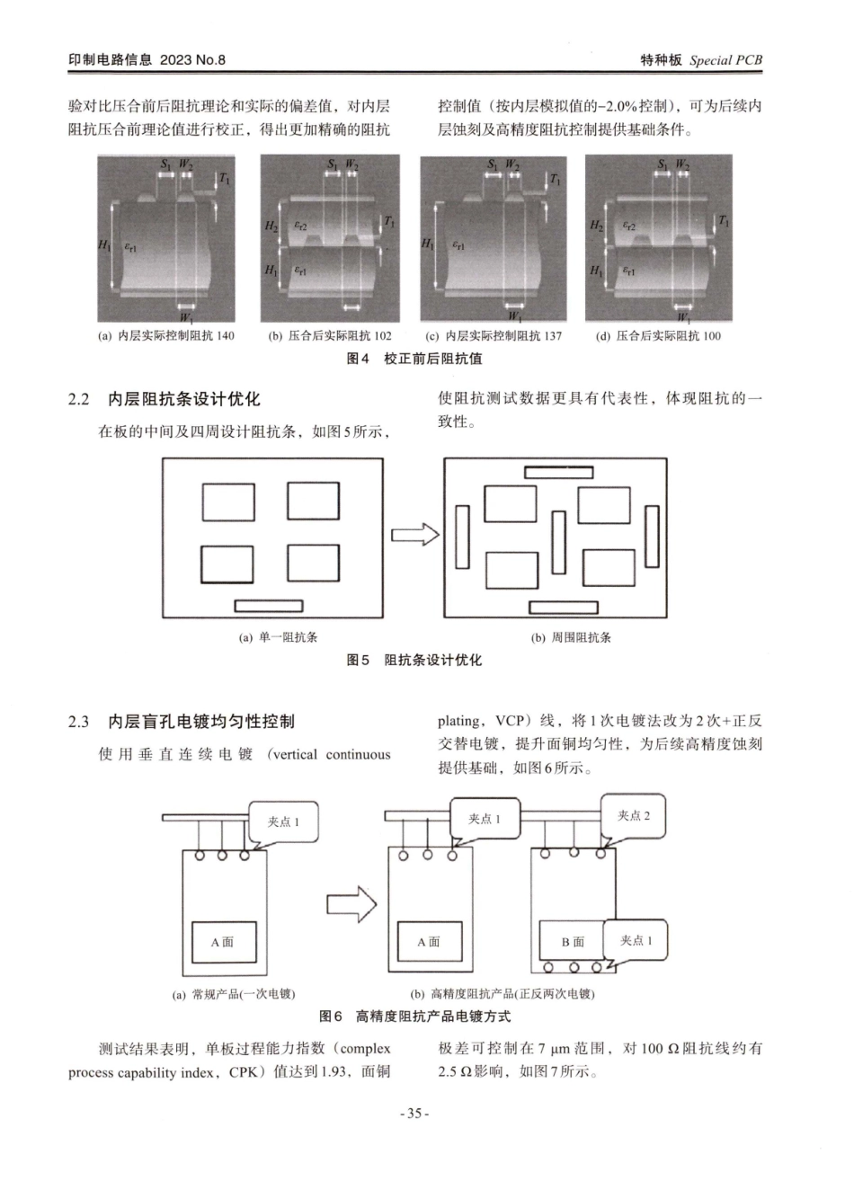
-33-印制电路信息2023No.8特种板SpecialPCB5G通信PCB高精度阻抗控制研究杨帆1,2唐宏华1,2樊廷慧1,2王斌1,2(1.惠州市金百泽电路科技有限公司,广东惠州516083;2.深圳市金百泽电子科技股份有限公司,广东深圳518049)摘要5G通信对信号完整性提出更严格的要求,因此对印制电路板(PCB)阻抗控制精度的要求也越来越高。内层阻抗受盲孔电镀、蚀刻一致性及压合前不易探测等因素影响导致出现偏差,超出土5%的管控标准。对此类高速产品的内层高精度阻抗控制技术进行研究,从不同铜厚控制、线宽线距、蚀刻工艺及阻抗检测方法等方面入手,通过工艺验证找出最优加工方案,实现内层阻抗土5%的高精度加工目标。关键词5G通信;印制电路板;阻抗控制;铜厚;线宽中图分类号:TN41文献标志码:A文章编号:1009-0096(2023)08-0033-05ResearchonhighprecisionimpedancecontrolofPCBfor5GcommunicationYANGFanl:2TANGHonghual.2FANTinghuil.2WANGBinl,2(1.HuiZhouKingBrotherCircuitTechnologyCo.,Ltd.,Huizhou516083,Guangdong,China;2.ShenZhenKingBrotherElectronicsTechnologyCo.,Ltd.,Shenzhen518049,Guangdong,China)Abstractt5Gcommunicationputsforwardmorestringentrequirementsforsignalintegrity,andasaresult,therequirementsforprintedcircuitboard(PCB)impedancecontrolaccuracyaregettinghigherandhigher.Duetoblindholeplating,etchingconsistency,anddifficultytodetectbeforepressing,theinnerlayerimpedanceispronetodeviation,exceedingthecustomer'scontrolstandardof±5%.Thisarticleistostudythehigh-precisionimpedancecontroltechnologyoftheinnerlayerofsuchhigh-speedproducts,fromdifferentsettingsofcopperthicknesscontrol,linewidthandlinespacing,etchingprocess,impedanceinspectionmethodsandotheraspects.Finallytheoptimalprocessingschemeisfoundthroughprocessverification,soastomeetthehigh-precisionprocessingrequirementsoftheinnerlayerimpedanceof±5%.Keywords5Gcommunication;printedcircuitboard(PCB);impedancecontrol;copperthickness;linewidth0引言在印制电路板(printedcircuitboard,PCB)行业中,5G类高速产品的信号传输速度越来越快,频率越来越高,对PCB的阻抗控制精度要求也越来越高。控制不严格的阻抗会引发较大的信作者简介:杨帆(1998一),男,工程师,本科,主要研究方向为新技术、新产品的开发及PCB...